In a significant leap for India's semiconductor sector, Union Ministers Ashwini Vaishnaw and Dharmendra Pradhan have inaugurated the country's first advanced 3D chip packaging unit in Bhubaneswar. This state-of-the-art facility is poised to bolster India's position in the global semiconductor supply chain, a strategic move amid increasing geopolitical tensions and supply chain disruptions worldwide. The unit is expected to produce 70,000 glass panels annually, alongside 50 million assembled units and approximately 13,000 advanced 3DHI modules. This development is not just a technological milestone but also a potential catalyst for economic growth in the region, offering new employment opportunities and attracting foreign investment. The Indian government has been actively promoting the semiconductor industry as part of its 'Make in India' initiative, aiming to reduce dependency on imports and enhance self-reliance. With the global semiconductor market projected to reach $1 trillion by 2030, India's entry into advanced chip packaging could open new avenues for collaboration with international tech giants. Investors and industry stakeholders are keenly observing how this facility will impact India's semiconductor landscape, potentially driving innovation and competitiveness in the tech sector.
business
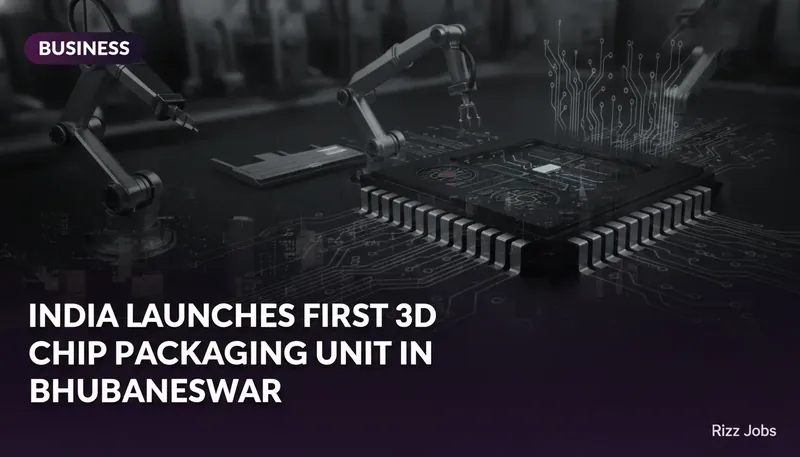
India Launches First 3D Chip Packaging Unit in Bhubaneswar
Rizz Jobs News Desk··1 min read
Market Briefing
- India's first advanced 3D chip packaging unit has been launched in Bhubaneswar, marking a major step in the country's semiconductor ambitions.
- The facility aims to enhance India's role in the global tech supply chain.
Share this story
Topics
3D chip packagingBhubaneswar techsemiconductor industryMake in Indiaglobal supply chain
Stay Informed
India's financial news, delivered daily.
Finance, markets, economy and startup updates — straight to your inbox.
Subscribe Free →

